top of page


The smart path to chiplets using hierarchical device planning and pin regions
Advancements in IC packaging manufacturing, combined with the exploding costs of designing monolithic ICs on today’s advanced process nodes, have given rise to a growing trend of disaggregating large SoCs into smaller dies and chiplets. This increased design complexity requires iterative multi-physics analysis during the floorplanning stage and optimization of the design for PPA and cost goals, significantly raising the barrier for project success. Trying to employ traditiona
Apr 30, 20241 min read


PCB design and analysis with PADS Professional Premium
Designing a printed circuit board can be a complex task if the application you are using does not provide the appropriate automation. Simplify the entire process by providing automation where it’s the most important. PADS Professional Premium delivers everything you need to design your simplest to most complex PCB designs. Full function, yet easy to use, with features and technologies like: Routing automation Can reduce PCB layout time by up to 80 percent. With electronics de
Jan 30, 20241 min read


PCB routing: art + automation
By Ray Macias and Gregory Beers PCB routing is one of the most enjoyable parts of PCB design , but also the most time consuming. It may take only a week to layout your board, but it could take you three months to route it unless you have the appropriate automation tools. PCB routing technology is more advanced than in years past, and yet, you can still be very creative and make a beautiful design. It makes sense to take advantage of the tools that are available to you when ro
Jan 16, 20244 min read


Navigating the maze of PCB routing: understanding interactive, auto, and sketch routing techniques
By Stephen Chavez In the world of PCB design, PCB routing plays a pivotal role in ensuring the efficiency and functionality of electronic circuits. Let’s explore the various PCB routing techniques, and shed some light on interactive routing, auto routing, and the empowering realm of sketch routing. Interactive routing: mouse-driven precision Interactive routing, the standard approach adopted by PCB designers across various PCB design tools, involves meticulous control over t
Jan 2, 20243 min read


Simplifying component research for efficient electronics design
By Matt Walsh Let’s delve into the challenges that electronic systems development organizations face and how an integrated part research solution, such as PartQuest Portal, can help streamline the design process, making it faster and more efficient. Challenges in electronics development Electronic systems development organizations are no strangers to complex challenges. Tight deadlines, resource limitations, the aspiration for first-pass success, and productivity hurdles coll
Dec 19, 20233 min read


PCB design best practices: electrical/electronic co-design
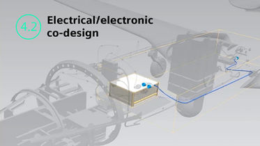
By Stephen Chavez What is electrical/electronic co-design? Circuit boards don’t work in isolation, they usually interface with other circuit boards via connectors, cables or harnesses. Electrical/electronic co-design is the integrated collaboration between these disciplines. This way, your entire hardware design from multi board electronic system specification to completed PCBs and cables can be handled within one integrated flow. What’s not working? Full systems design is us
Nov 21, 20232 min read


Frequently asked questions about PADS Professional
By Jim Martens You asked and we answered! Here are the frequently asked questions about PADS Professional. What is PADS PCB design software? PADS PCB software is a comprehensive electronic design automation (EDA) software suite developed by Siemens Digital Industries Software, formerly Mentor Graphics. It provides advanced tools for designing, simulating, verifying, and manufacturing printed circuit boards (PCBs) and electronic systems. What does PADS Professional include? PA
Oct 24, 20234 min read


What’s new in PADS Professional release VX.2.12
By Jim Martens The new VX.2.12 release of PADS Professional has improvements across the following areas: Array placement MCAD collaborator Physical reuse Improved differential pair stability while moving complex vias High speed routing and design Performance General improvements PADS Professional cloud ecosystem applications Array placement We have made some design creation improvements that affect predictability such as the new array component property, and we have improved
Oct 18, 20223 min read


PADS Standard 進階佈局設計實戰課程 圓滿結束
PADS 是用來設計線路圖和 PCB 的專業軟體,全球市佔率超過50%,本次【PADS Standard 進階佈局設計實戰課程】,邀請有豐富業界實務經驗的資深 AE 工程師,針對電路圖繪製、電路板佈局佈線設計、佈線技巧以及電路板製造設定及文件等關鍵實戰應用進行講解,幫助學員快速掌握設計重點與技巧。 紮實的課程內容,不僅以深入淺出的方式教導學員,同時透過現場實作,讓每位學員實地操作,如何以最有效率的方式進行設計,本次課程也在熱烈的討論中圓滿落幕,相信學員們都 滿載而歸! 同時近期收到許多課程資訊的詢問,目前9月份課程已開放報名,歡迎索取課程資訊,帶您快速從入門到精通,快速加強 PCB 設計實力! 恩萊特科技股份有限公司 Enlight Technology Co., Ltd. www.enlight-tec.com 300052 新竹市東區關新路27號14樓之1 電話:03-602-7403 傳真:03-563-0016 sales@enlight-tec.com
Jun 28, 20221 min read
bottom of page
