top of page


How to get accurate inductance extraction for superconductor ICs
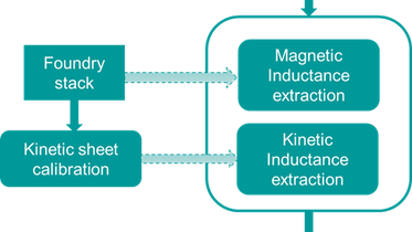
By Hossam Sarhan and Dusan Petranovic Supporting the high performance and reliability needed for artificial intelligence (AI), data centers and cloud computing requires powerful and efficient integrated circuits (ICs). More semiconductor companies are considering superconductor ICs for their unique properties that allow ultrafast processing of digital information. These properties include fast superconducting transmission lines and active devices called Josephson junctions, w
Aug 27, 20243 min read


Using a shift left strategy to address block/chip design challenges during design-stage verification
By David Abercrombie For IC designers, striking the right balance between tight deadlines and limited resources is a constant challenge. Designers are constantly working to enhance efficiency without compromising on design quality. Traditionally, IC design and verification followed a linear process, but modern IC designs require a more concurrent approach that addresses block/chip layout and circuit issues earlier in the design flow. A new approach that provides signoff-quali
Aug 20, 20243 min read


Unlocking the future with a digital twin for semiconductor manufacturing
By Srividya Jayaram In semiconductor manufacturing, staying ahead means embracing smarter processes. The rise in demand and the need to maximize profits call for innovative solutions to improve yield ramp for new products. Siemens, a pioneer in digital twin technology in multiple industries including energy, factory automation, and aerospace now extends this solution to the electronics and semiconductor manufacturing industry with the Calibre Fab Insights platform. This platf
Aug 13, 20244 min read


How to verify well layer connectivity with soft checks
By Terry Meeks In the landscape of modern IC chip verification, ensuring the connectivity from diffusion layers to well regions is...
Aug 6, 20244 min read


A new physical verification reporting solution smooths the on-time tapeout effort
By Richard Yan In the intricate world of system-on-chip (SoC) development, Physical Verification (PV) reports serve as vital checkpoints...
Jul 30, 20242 min read


Balancing performance vs. debuggability in LVS circuit verification
By Wael ElManhawy Circuit verification engineers face ever more challenges as semiconductor technology evolves towards smaller process...
Jul 23, 20243 min read


Speeding up early design rule checking with Calibre nmDRC Recon
By John Ferguson and Nermeen Hossam Chip designers are very aware of how time-consuming early design rule checking (DRC) can be. Not only that, but traditional DRC runs during initial design phases can flood you with errors that may be irrelevant at this early stage. Sorting through these is a massive drain on time that you don’t always have. So let’s talk about Calibre® nmDRC™ Recon, a tool that makes early design rule exploration faster and more efficient. What is Calibre n
Jul 16, 20243 min read


Automated analysis-based layout enhancements reduce power grid voltage drops during place & route: A case study with Google
By Jeff Wilson Power isn’t just a small factor in the IC design arena—it’s a cornerstone. Design teams work to hit the trifecta of power, performance, and area (PPA) targets that reflect the intended market and functionalities of their products. The journey from concept to physical implementation is one of precision and innovation, as these teams shape layouts that meet these stringent targets. But, as technology pushes into more advanced process nodes, striking a balance bet
Jul 9, 20243 min read


Accelerate IP design cycles and reduce costs with Calibre design stage verification
By Terry Meeks In the fast-paced world of semiconductor design, time is a critical asset. One way IC designers save time is to...
Jun 25, 20244 min read
bottom of page
